Explore our state-of-the-art printed circuit boards, server CPU coolers, memory interfaces, and custom flexible circuit configurations.
An in-depth analysis of materials, thermal efficiency, global supply chain paradigms, and advanced hardware manufacturing technologies.
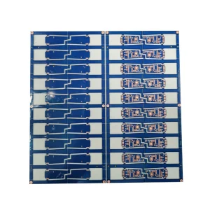
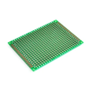
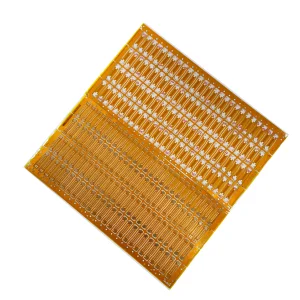
The global electronics sector relies heavily on the mechanical stability and electrical routing integrity of printed circuit boards (PCBs). Single-sided and double-sided PCBs constitute the foundation of this ecosystem, providing structural support and layout routing for consumer appliances, industrial machinery, and telecom hardware. As modern designs require smaller dimensions and higher frequencies, selection of the appropriate board design is critical. Single-sided PCBs utilize a single conductive copper layer laminated to a rigid insulating substrate, whereas double-sided PCBs use both sides of the dielectric core, interconnected via Plated Through-Holes (PTH). Choosing between single and double-sided architectures involves evaluating mechanical complexity, thermal requirements, signal frequencies, and manufacturing costs.
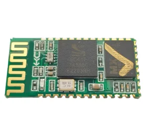
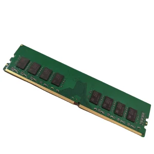
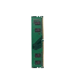
Xeviora Memory Technology (China) Co., Ltd. stands as a key partner in this tech landscape. While specializing in high-performance DDR5 memory systems, gaming RAM, and industrial storage modules, Xeviora integrates advanced PCB engineering into its processes. Established in 2017, the company combines 12 years of industry experience with 8 years of international export logistics. Working from a specialized 368-square-meter facility with an annual export value exceeding USD 18 million, Xeviora maintains strict design-for-manufacturability (DFM) rules. This guarantees high-yield production runs for double-sided PCBs, memory substrate systems, and specialized sub-assemblies.
High-frequency operations demand advanced base laminates. For example, aluminum substrate boards coated with high-performance copper foils or Taconic TLY-5 (0.254mm) PTFE substrates are used to minimize signal attenuation and dielectric loss. Selecting these materials is essential for high-frequency telecommunication hardware, high-power LED systems, and specialized detectors requiring high signal integrity.
The technology path for single and double-sided PCBs is defined by three trends: layout miniaturization, ecological material adaptation, and hybrid circuit integration. With the growth of Internet of Things (IoT) hardware and wearable medical systems, the demand for thin, light, and durable circuits has increased significantly.
Traditional subtractive etching is shifting toward Semi-Additive Processing (mSAP). This change allows trace widths and spacing to decrease from 100μm to below 30μm, enabling high-density routing on standard two-layer substrates.
Standard FR4 is being replaced by high-glass transition temperature (High Tg) epoxy resins, Polyimide, and PTFE. These materials maintain thermal and mechanical stability under high-speed data transmission and high temperatures.
The manufacturing process is adopting green chemistries, lead-free surface finishes (such as ENIG and OSP), and halogen-free base laminates to comply with global environmental regulations.
Analyzing current global demand alongside specific, regional engineering applications.
The global demand for printed circuit boards is driven by regional industrial specializations. In North America and Europe, the focus centers on aerospace, military electronics, medical systems, and high-performance server farms. These industries require reliable double-sided PCBs, such as server motherboard substrates that handle thermal expansion well. In contrast, the market in Southeast Asia and South America is driven by consumer electronics, automotive assemblies, and home appliances, which require cost-effective single-sided PCBs or flexible polyimide circuits.
By studying specific local application scenarios, engineers can select the correct materials and design rules for their boards:
Why Chinese manufacturing hubs offer unmatched advantages in logistics speed, material access, and production scale.
The Chinese PCB supply chain provides high efficiency, material availability, and production capacity. Guangdong and surrounding electronics clusters house complete networks for raw materials, copper-clad laminates (CCL), chemical suppliers, high-precision CNC drillers, and automated assembly plants. This concentration reduces lead times and allows manufacturers to scale production quickly from initial prototype to volume delivery.
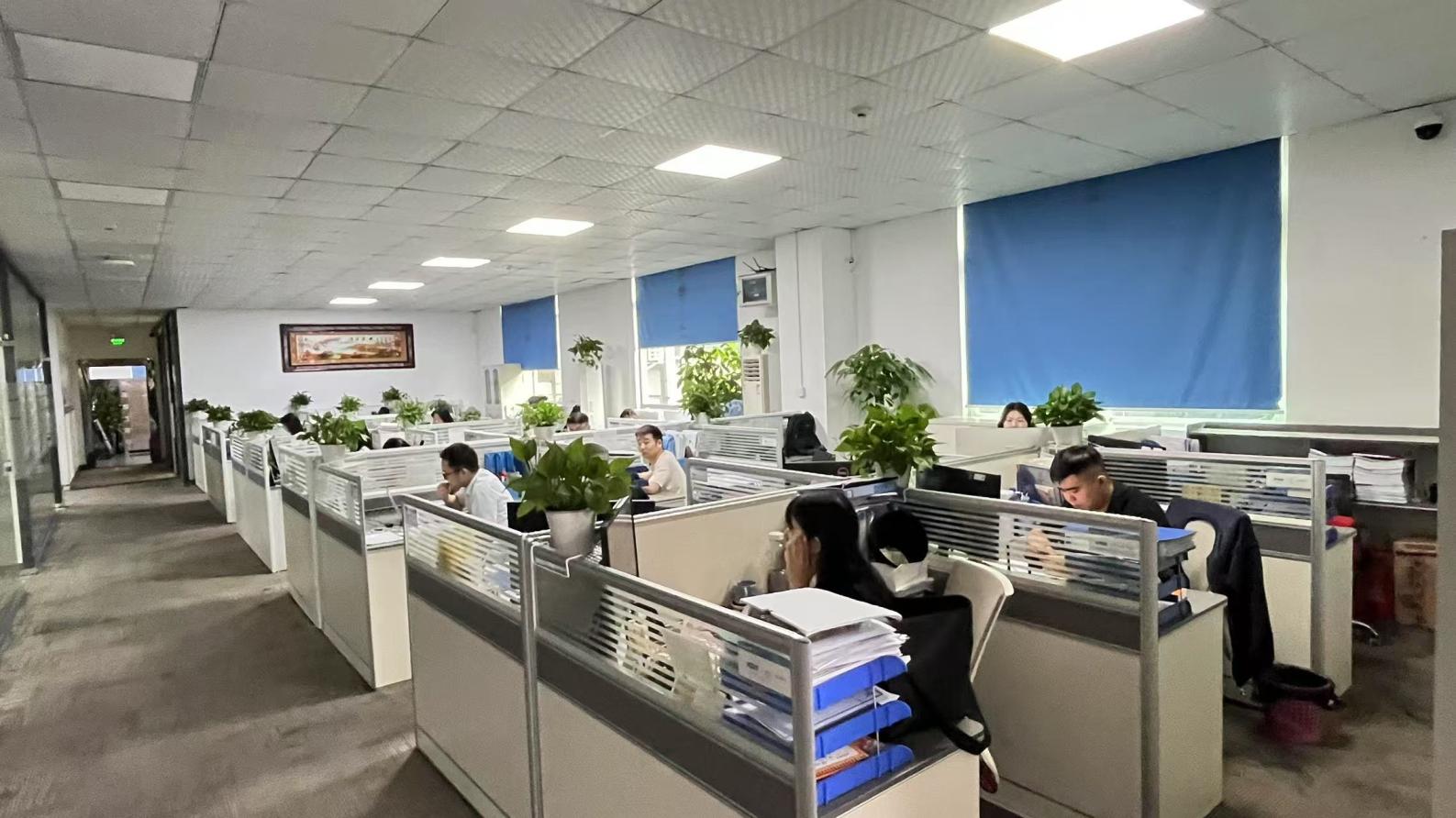
Xeviora leverages this regional ecosystem to build a resilient supply chain. Collaborating with over 850 vetted supply chain partners worldwide, Xeviora ensures access to raw materials and components, even during market fluctuations. Supported by an experienced R&D team of 128 engineers, Xeviora handles design-for-assembly (DFA) reviews and customized prototyping. This team launched 86 new memory and circuit products last year, demonstrating our design agility. The engineering team manages complex PCB layups, layout optimizations, and thermal designs, helping customers transition from product concept to finished circuit boards.
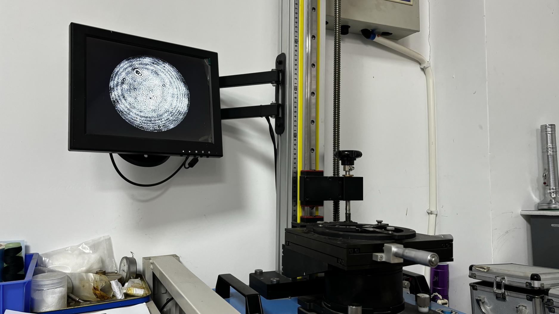
A quality assurance team of 46 dedicated inspectors monitors the manufacturing flow. The QA process includes incoming material inspection (IQC), in-process quality control (IPQC), final automated testing (FQC), and thermal stress testing. Every batch of double and single-sided boards undergoes electrical continuity testing, solderability checks, and surface layer audits to ensure long-term field reliability.
Ensuring your products meet global regulatory frameworks and quality benchmarks.
Global electronics markets require strict compliance with safety, environmental, and engineering standards. Industrial and automotive systems require PCB suppliers to hold valid certifications to guarantee safety and performance. Xeviora manages regulatory compliance across different target markets to ensure smooth export clearance:
Additionally, Xeviora offers localized support to system builders, distributors, and brand owners. By providing direct engineering communication, hardware customization, packaging design, and firmware tuning for memory modules, we help customers minimize time-to-market and resolve technical issues quickly.
Professional engineering answers to key technical questions about single and double-sided PCBs.
A single-sided PCB has conductive copper tracks on only one side of the insulating dielectric board, making it ideal for simpler, low-cost applications. A double-sided PCB has copper layers on both sides, using plated through-holes (PTH) to route electrical connections between layers. This layout allows for more complex, higher-density component placing.
Taconic TLY-5 is a PTFE-based substrate reinforced with woven fiberglass, featuring a low dielectric constant (Dk) of 2.2 and a dissipation factor of 0.0009 at 10GHz. This material chemistry minimizes dielectric loss and signal distortion, making it a reliable choice for RF, microwave, and high-speed data transmission systems.
Aluminum substrate PCBs consist of a metal base plate, a thin, highly thermally conductive dielectric layer, and a standard circuit copper foil. The aluminum core transfers heat away from critical, heat-generating components (such as power transistors or LEDs) much faster than standard FR4, preventing thermal failures.
Due to the proximity of component suppliers, raw materials, and packaging manufacturers in our electronics cluster, typical prototyping takes 3 to 5 working days, while bulk commercial production runs are completed in 10 to 15 days, depending on compliance and surface finish requirements.
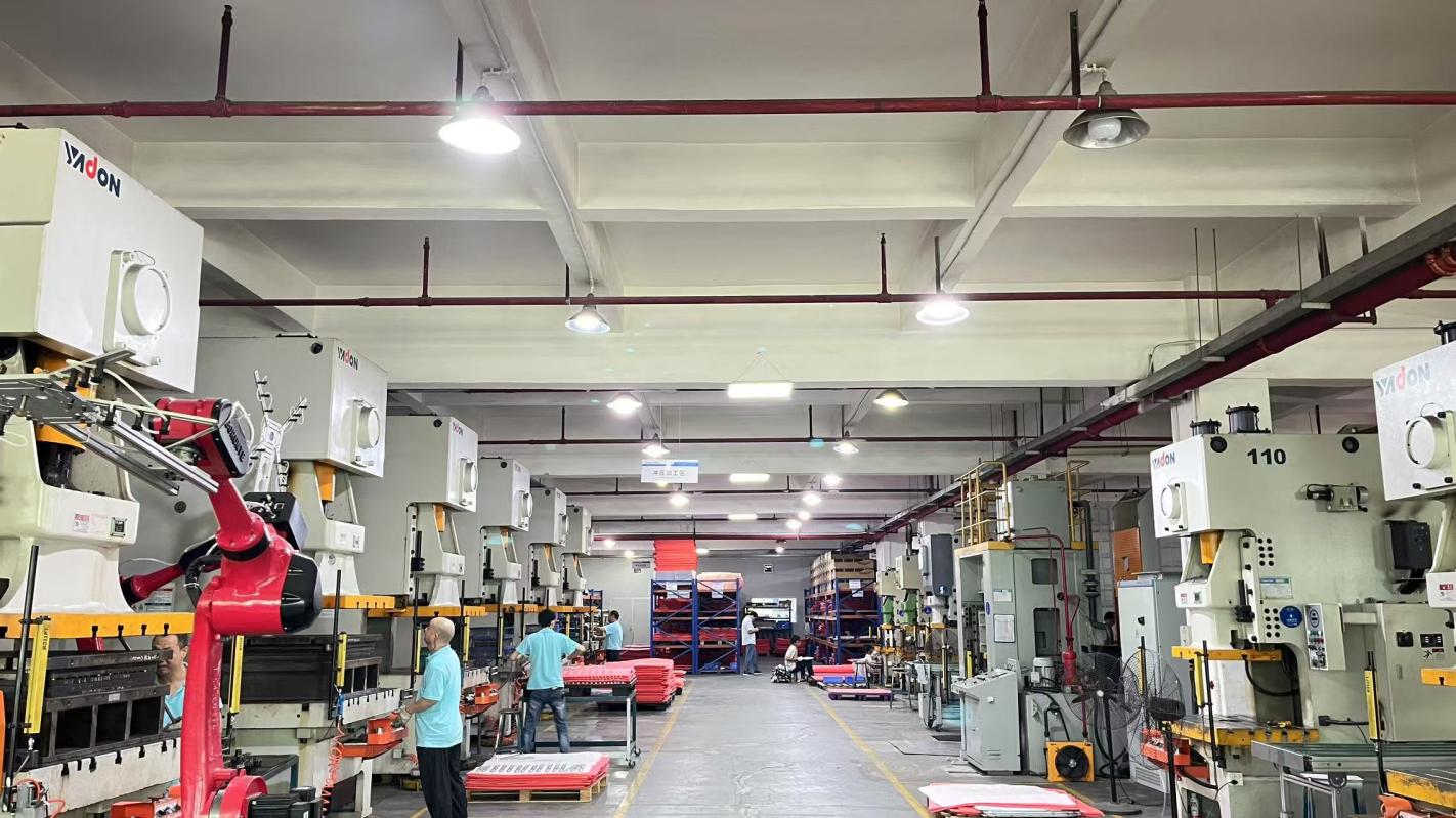
A look inside our manufacturing floor, cleanroom spaces, quality checkpoints, and advanced assembly lines.

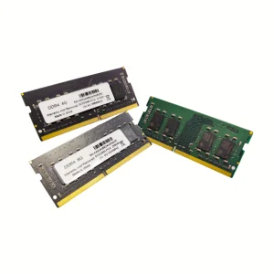
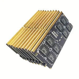
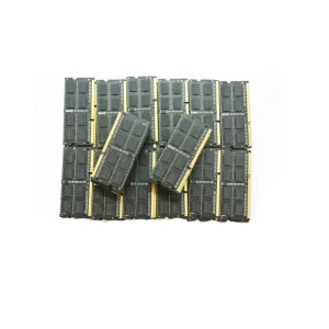
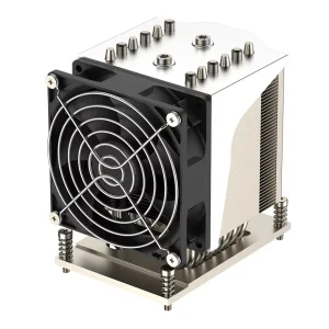
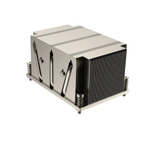
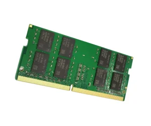
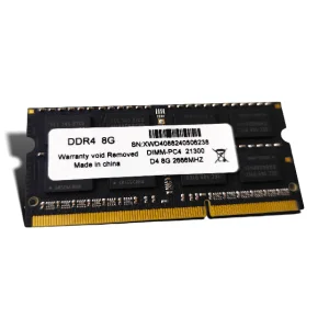
High-performance DDR RAM, processing heatsinks, and core memory components optimized for complex systems.