Direct access to our engineered-to-spec printed circuit boards, micro-assemblies, and high-performance server architectures configured for Japan's industrial sectors.
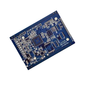
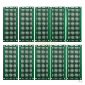
As Japan's historic powerhouse of precision engineering and mechanical innovation, the Kansai region (centered around Osaka, Kyoto, and Kobe) remains a global hub for advanced robotics, medical instrumentation, automotive electronics, and high-frequency communication modules. Companies in Osaka operate under strict quality paradigms where component failure is not an option. From the dense micro-vias required in high-density interconnect (HDI) substrates to heavy-copper power circuit boards for factory automation, local engineering requirements call for high thermal resilience, precise impedance control, and reliable chemical finishes.
Osaka’s local prototype shops excel at NPI (New Product Introduction) and fast local engineering support. However, scaling these high-density multi-layer designs to high-volume commercial production requires international synergy to balance unit costs and capacity demands.
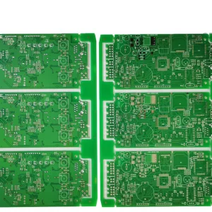
Global electronics demand requires agile factories capable of producing High-Mix Low-Volume (HMLV) batches. By coordinating design schematics in Japan and executing precision fabrication in highly-automated Chinese cleanrooms, procurement teams achieve superior unit economics.
Modern procurement strategies depend on flexible vendor pipelines. Diversifying fabrication across reliable partners reduces geopolitical bottlenecks, ensuring consistent flow of essential PCBs, surface-mount components, and heat sinks.
| Procurement Parameter | Osaka Local Prototyping Facilities | High-Volume Offshore Partners (e.g., Xeviora China) | Strategic Synergy Recommendations |
|---|---|---|---|
| Turnaround Time | 24 - 48 Hours (Ultra-fast local delivery) | 5 - 9 Working Days (Including air logistics) | Develop prototypes in Osaka; immediately push finalized Gerbers to China for scale run. |
| Cost per Board (Multilayer) | High (Premium local labor and tooling setup) | Highly Competitive (Optimized supply chain & materials) | Consolidate raw material acquisition and sheet processing with offshore automated plants. |
| Technical Layer Limits | Typically up to 16 Layers for fast-turnaround | Up to 64 Layers (High-density HDI, blind/buried vias) | Leverage massive offshore facilities for high-complexity, micro-via server backplanes. |
| Component Sourcing (PCBA) | Limited local distribution inventories | Direct access to global component and memory suppliers | Deploy hybrid assembly to bypass global component allocation and chip shortages. |
Modern high-performance compute nodes, industrial edge-AI devices, and automated machinery in Osaka demand more than just raw bare boards. They require a holistic approach to sub-system integration. A printed circuit board is only as good as the active silicon, memory modules, and thermal dissipation systems mounted to it.
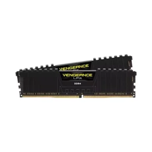
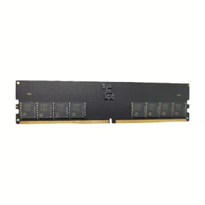
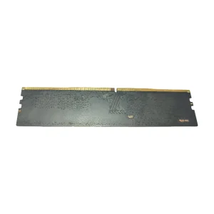
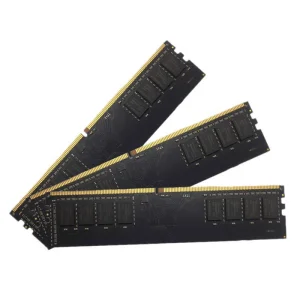
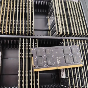
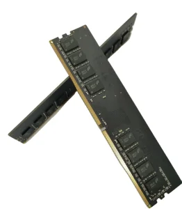
In applications such as machine vision (used extensively in Osaka's sensor industry), processing latency must be minimized. This requires mounting DDR4 or DDR5 RAM directly onto CPU-adjacent PCBA layers or utilizing robust SO-DIMM/ECC slots. Standard consumer memory modules cannot withstand the vibrations and thermal stress of factory floors. Industrial-grade ECC memory (Error-Correcting Code) ensures that bit flips caused by electromagnetic interference (EMI) do not shut down continuous automated production lines.
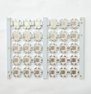
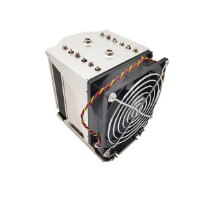
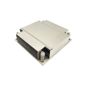
Furthermore, high-speed memory and high-power processors generate massive heat density. Proper PCB layout must incorporate thick copper planes, thermal vias, and specialized substrates such as Aluminum PCBs (e.g., T6 5050/3535 lamp bead substrates) to direct heat away from delicate active components. In server-level PCBA designs, this integration is completed by heavy-duty 320W LGA4189 air-cooled heat sinks or extruded aluminum radiators, preventing thermal throttling and extending the operational lifespan of the entire system.
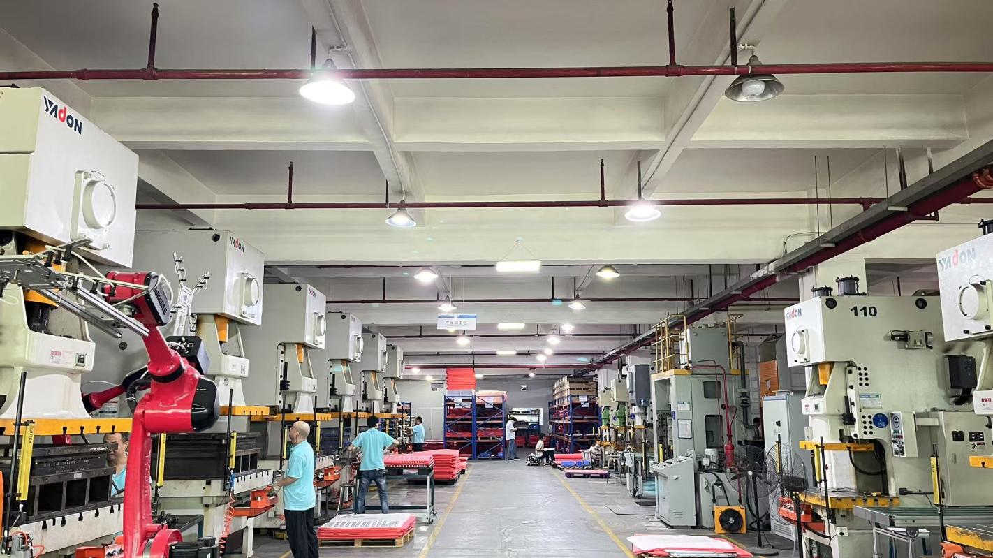
As a key OEM and ODM manufacturing partner, Xeviora Memory Technology (China) Co., Ltd. specializes in the fabrication and assembly of high-density memory modules, server computing boards, and related thermal components. Established in 2017, we have scaled our operations to support clients in North America, Europe, Southeast Asia, and industrial markets in Japan, generating an annual export revenue exceeding USD 18 million.
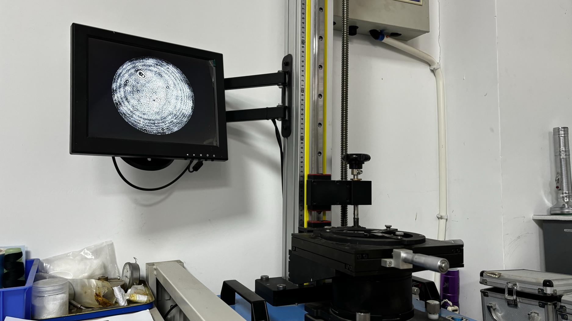
Our specialized production cleanrooms, equipped with advanced automatic placement machines and automated optical inspection (AOI) setups, focus on high-precision and high-speed assembly processes. Every single memory module and printed circuit assembly is subjected to a rigorous QA sequence:
Whether you require standard DDR4/DDR5 SO-DIMMs for localized embedded systems or custom multilayer PCBA with specific thermal management components, our R&D team of 128 engineers provides full design-for-manufacturability (DFM) reviews to prevent field failures.

Addressing critical engineering and logistical questions for Osaka and international technology procurers.
Yes. Our engineering division of 128 personnel provides customized firmware optimization, SPD programming, specialized form factors, and unique thermal spreader designs. We run prototype compatibility checks on key local platform brands prior to serial delivery.
HASL (Hot Air Solder Leveling) provides excellent solderability and shelf life, which is ideal for standard 2-layer configurations. For high-frequency, fine-pitch SMT assembly (such as memory modules or complex industrial controllers), we recommend Immersion Silver or ENIG to achieve a perfectly flat, coplanar pad surface and prevent signal loss.
All our raw materials, copper-clad laminates, chemical reagents, and solder alloys comply strictly with European RoHS and REACH directives, which align with green procurement standards in Japan. Third-party testing certifications are supplied with every dispatch batch.
We maintain streamlined shipping corridors. Air freight from our facilities to Kansai International Airport (KIX) typically takes between 2 to 4 business days. For volume manufacturing orders, sea freight schedules to the Port of Osaka are arranged for cost efficiency.
We recommend deploying our 320W LGA4189-N96 multi-pipe heat sink configurations with low-resistance thermal interface materials (TIM). Thermal routing calculations should always be verified using detailed computational fluid dynamics (CFD) simulation models.
Select from our specialized line of server memory upgrades, copper substrate PCBs, high-speed RAM components, and high-efficiency thermal dissipators.
Connect with our expert engineering team to submit your Gerber files, review layer configurations, and secure scalable volume quotes tailored for Osaka's demanding industrial standards.
Send Inquiry Now