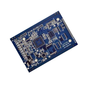
Essential components customized for Thailand's automated smart manufacturing and computing systems.
The Bangkok metropolitan area, spanning provinces like Samut Prakan, Pathum Thani, Ayutthaya, and stretching into the Eastern Economic Corridor (EEC) zones of Chonburi and Rayong, has transformed into a global powerhouse for advanced electronics manufacturing. Historically recognized as a premier location for hard disk drive (HDD) manufacturing, the region is undergoing a structural shift toward smart electronics, electric vehicles (EVs), renewable energy power electronics, and industrial automation control systems.
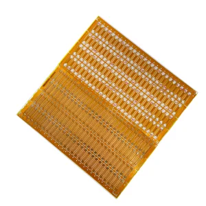
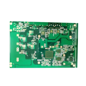
As multinational corporations establish deep-tier manufacturing plants in Thailand, the demand for precision surface mount technology (SMT) has escalated. High-density SMT processes rely on a crucial interface: the SMT Laser Stencil. A laser stencil is the foundational template that governs the deposition of solder paste onto printed circuit boards (PCBs). In an environment where micro-components such as 0201 and 01005 passives, ultra-fine-pitch Ball Grid Arrays (BGAs), and Quad Flat No-leads (QFN) packages are standard, stencil accuracy is directly proportional to final product yield.
Manufacturers in Bangkok face unique local operating realities, including high relative humidity, which impacts solder paste rheology and stencil release characteristics. To counter these environmental variables, SMT engineers must partner with advanced laser stencil manufacturers capable of delivering nano-coated stencils, electroformed foils, and stepped stencil designs that accommodate mixed-technology boards. The regional transition from labor-intensive manual assembly to fully automated Industry 4.0 production lines makes stencil precision the absolute key to minimizing defects like bridging, solder balls, and voiding.
The core challenge of SMT stencil printing lies in the fluid dynamics of solder paste transfer. As apertures shrink to accommodate modern microprocessors and memory modules, simple gravitational release of the paste is no longer sufficient. The performance of a laser-cut stencil is governed by the Area Ratio and Aspect Ratio rules:
Area Ratio (AR) Formula:
AR = Area of Aperture Opening / Area of Aperture Walls = (W × L) / (2 × (W + L) × T)
* For standard apertures, maintaining an Area Ratio > 0.66 is critical to achieve an acceptable transfer efficiency (over 70% paste release). For high-performance electronic designs, special nano-coatings or electroformed stencils are deployed to push the physical threshold down to 0.50.
To meet these constraints, state-of-the-art laser stencils leverage several engineering options:
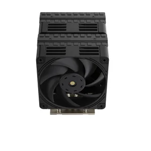
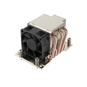
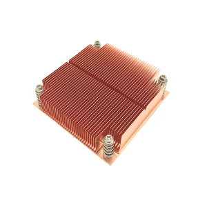
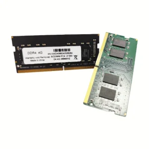
Precision thermal management and high-frequency memory modules optimized for industrial computing.
For modern electronic manufacturing services (EMS) in Thailand, relying strictly on domestic stencil production can sometimes introduce supply bottlenecks, especially when handling complex high-layer count boards, step-stencil variations, or specialty nickel-electroformed tooling. Sourcing from a partner embedded in China’s advanced Industry 4.0 manufacturing cluster offers substantial resilience, scalability, and quality guarantees.
The Chinese electronics ecosystem operates at an unprecedented level of integration. From raw high-tensile stainless steel foil manufacturing to automated laser calibration systems, every step is optimized. China's intelligent manufacturing framework leverages:
A global leader in high-performance computing hardware, industrial-grade storage solutions, and SMT manufacturing partnerships.
Xeviora Memory Technology (China) Co., Ltd. is a professional DDR5 memory manufacturer and supplier based in China, specializing in high-performance RAM solutions for gaming, industrial, enterprise, and consumer applications. Established in 2017, the company has rapidly grown into a trusted OEM and ODM partner for global distributors, system integrators, and technology brands.
Our manufacturing facility covers 368 square meters and is equipped with advanced production and testing equipment to ensure stable quality and reliable performance. With an annual export revenue of over USD 18 million, Xeviora serves customers across North America, Europe, Southeast Asia, the Middle East, and South America.
Backed by 8 years of export experience and 12 years of industry expertise, we are committed to delivering innovative memory products that meet international quality standards. Our quality management system includes comprehensive incoming material inspection, in-process quality control, and final product testing. All products undergo automated functional testing, compatibility verification, performance validation, and aging tests before shipment. Our quality assurance team consists of 46 dedicated inspectors who ensure every module meets strict reliability requirements.
As a manufacturer with strong OEM and ODM capabilities, Xeviora works closely with more than 850 supply chain partners worldwide, enabling efficient sourcing, flexible production, and fast delivery. Our primary customers include wholesalers, distributors, e-commerce sellers, system builders, brand owners, and enterprise solution providers.
Innovation is at the core of our business. Supported by an experienced R&D team of 128 engineers, we continuously invest in new technologies and product development. Last year alone, we successfully launched 86 new memory products covering DDR5 gaming memory, industrial-grade memory modules, server memory solutions, and customized storage products.
We offer flexible customization services, including private labeling, logo printing, packaging design, specification customization, firmware optimization, and complete OEM/ODM development. Whether customers require standard memory modules or fully customized solutions, our team is dedicated to providing reliable products, competitive pricing, and professional technical support.
At Xeviora, our mission is to empower global customers with advanced memory technology, dependable manufacturing, and long-term business partnerships built on quality, innovation, and trust.
Precision laser stencils and associated SMT processes operate at the heart of diverse industrial sectors across the Bangkok metropolitan region:
With the rapid adoption of Electric Vehicles (EV) and ADAS (Advanced Driver Assistance Systems) in Thailand, tier-1 suppliers require zero-defect PCBA. High-vibration automotive environments require thick step stencils to apply extra solder paste volume onto power connectors while keeping precision deposits for microprocessor control ICs.
Smart home appliances and solar inverter assemblies manufactured in Samut Prakan utilize complex double-sided reflow configurations. Stencil designs must optimize aperture aspect ratios for micro-sized Wi-Fi/Bluetooth communication modules to prevent bridging under high density conditions.
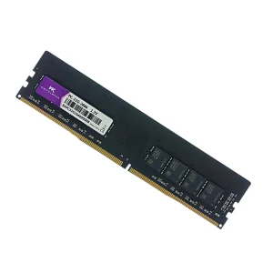
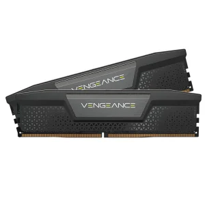
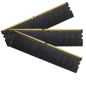
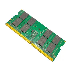
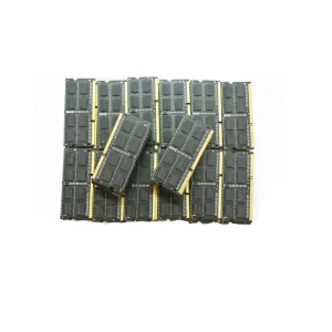
Bangkok's classic storage hubs are transitioning to server memory assemblies. High-frequency DDR4 and DDR5 memory modules necessitate incredibly tight tolerances. Electro-polished, nano-coated laser stencils ensure consistent solder volume release, preserving signal integrity across multi-gigabit traces.
Expert answers addressing the operational challenges and sourcing logistics of laser stencils for Thailand.
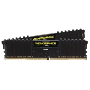
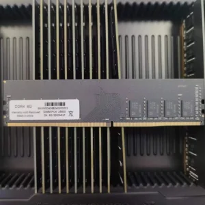
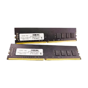
Enterprise and industrial grade memory modules engineered to support high-density processing environments.
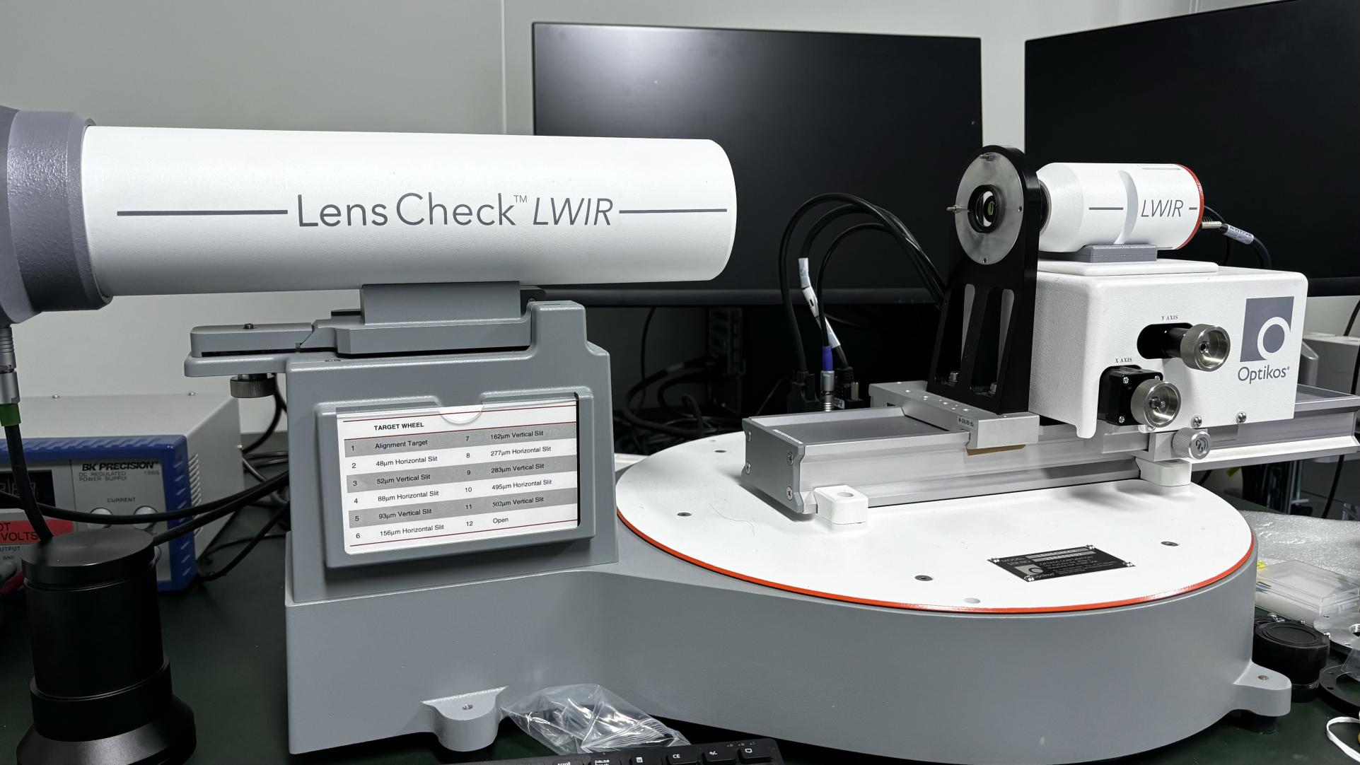
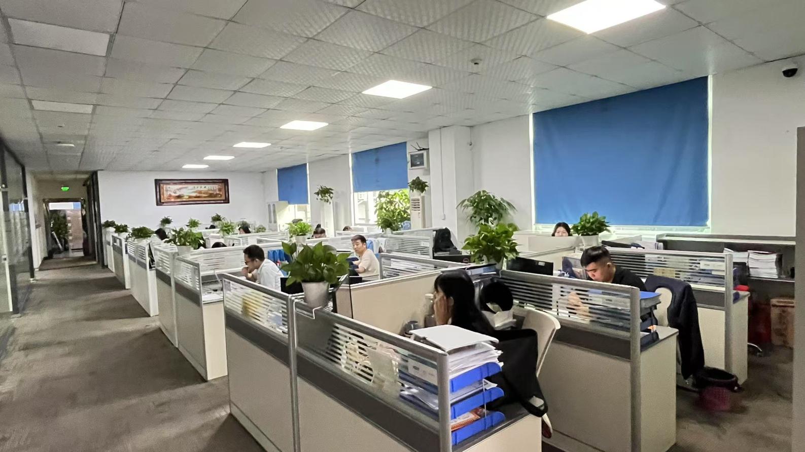
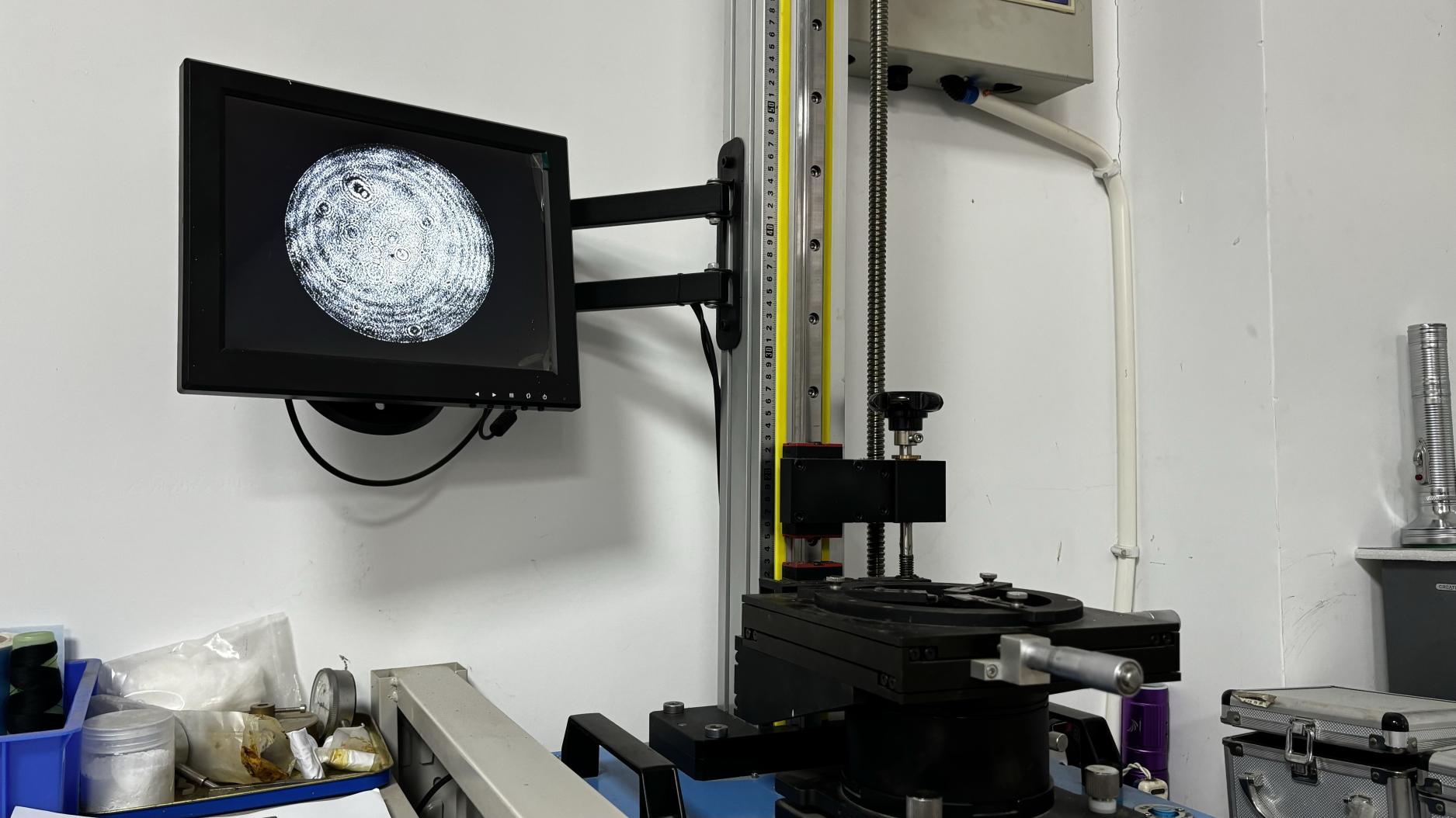
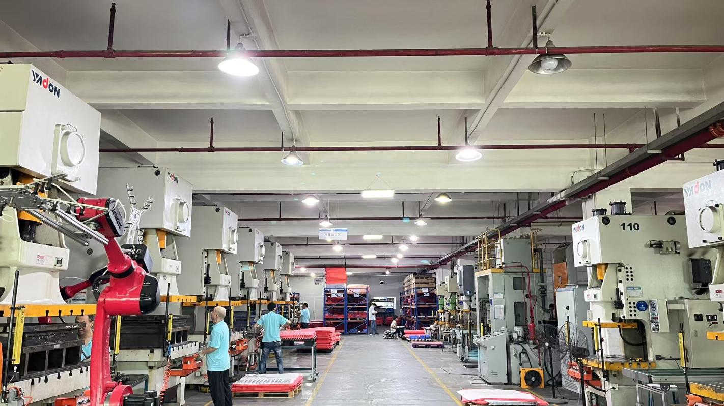
A glimpse into our advanced SMT laboratory, storage chip validation setups, and testing facilities.

Get in touch with our expert design engineers for stencil DRC analysis, custom aperture modifications, nano-coated foil solutions, or memory OEM/ODM supply agreements.