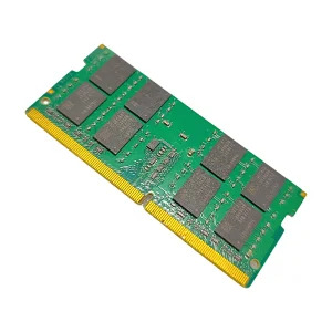
In modern high-performance computing, the boundaries between Digital Signal Processing (DSP), volatile memory access (DDR4/DDR5), and localized control circuit designs have collapsed. Xeviora Memory Technology (China) Co., Ltd. stands at the forefront of this convergence, operating as a leading OEM/ODM manufacturer specializing in high-speed data pathways, signal integrity, and robust system-level integration.
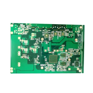
Established in 2017, we have scaled our research and engineering resources to design and build high-performance computing architectures. By utilizing advanced multi-layer printed circuit board (PCB) designs and embedding custom logic execution units, we ensure that digital signal pathways are optimized for ultra-low latency, maximum data throughput, and sustained stability under harsh electrical environments. Our facility spans over 368 square meters of state-of-the-art laboratory space and cleanroom production lines, allowing us to generate over USD 18 million in annual export revenue across key markets in North America, Europe, Southeast Asia, the Middle East, and South America.
Our operation is built on deep structural expertise. Armed with 12 years of industry engineering experience and 8 years of global export proficiency, we offer highly tailored ODM capabilities. This includes modifying system firmware, optimizing clock frequency management, routing high-density interconnect (HDI) PCBs, and executing high-level system-in-package (SiP) integration for custom DSP and computing units.
As computing needs shift towards real-time processing and edge AI execution, our digital signal processor architectures are evolving rapidly. We focus on integrating heterogeneous processing pipelines that bridge high-frequency arithmetic units with low-latency memory buses.
Integrating RISC-V hardware architectures alongside specialized MAC (Multiply-Accumulate) arrays to achieve maximum operations per watt in real-time sensor processing and audio stream decoding.
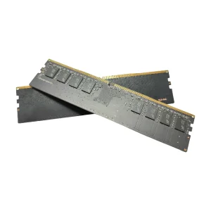
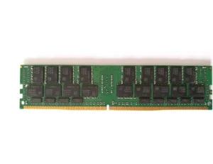
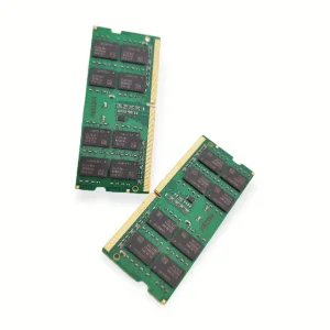
Directly embedding ultra-low-latency DDR4/DDR5 system interfaces directly with the processing package, avoiding conventional layout bottlenecks and optimizing the power envelope.
Integrating dedicated FP16/INT8 hardware accelerators into the DSP signal pipelines to execute predictive analysis and deep neural network interference at sub-millisecond latencies.
We deliver complete hardware ecosystems designed to survive and thrive in demanding macro-industrial environments.
| Industrial Application | Technical Challenge Solved | Hardware Implementation | Target Reliability Standard |
|---|---|---|---|
| Automotive & ADAS | Extreme temperature shifts & heavy EM interference. | AEC-Q100 certified components, high-efficiency aluminum alloy heat-sink coupling, and shielded multi-layer PCB design. | Zero-defect manufacturing, ISO 26262 ASIL-D. |
| Edge Telecommunications | Dense data packet handling at local base stations. | Multi-channel DSP modules coupled with high-frequency 6000MHz DDR5 arrays for dynamic packet switching. | NEBS Level 3 Compliance. |
| Industrial Smart Automation | Real-time feedback control loops in CNC and high-speed robotic arms. | Custom programmed FPGA/DSP hybrids with hard-coded floating-point mathematics cores. | 24/7 continuous operation under 65°C ambient. |
| Professional Audio & Imaging | High precision analog-to-digital signal fidelity. | Dedicated ultra-low noise floor power planes, isolated RF shield housings, and optimized low-jitter clock circuits. | THD+N < 0.0001% performance validation. |
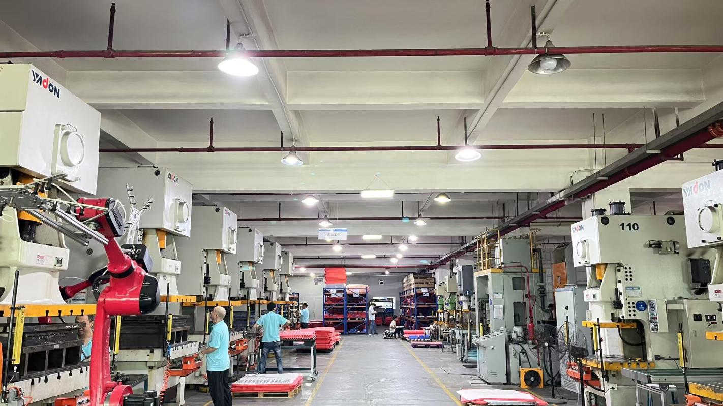
The core of our operational competitiveness is our integrated Chinese manufacturing environment. Leveraging the electronics ecosystem in the Pearl River Delta, Xeviora combines component sourcing speed, multi-stage Automated Optical Inspection (AOI), and precise high-speed Surface Mount Technology (SMT) lines to provide unmatched production elasticity.
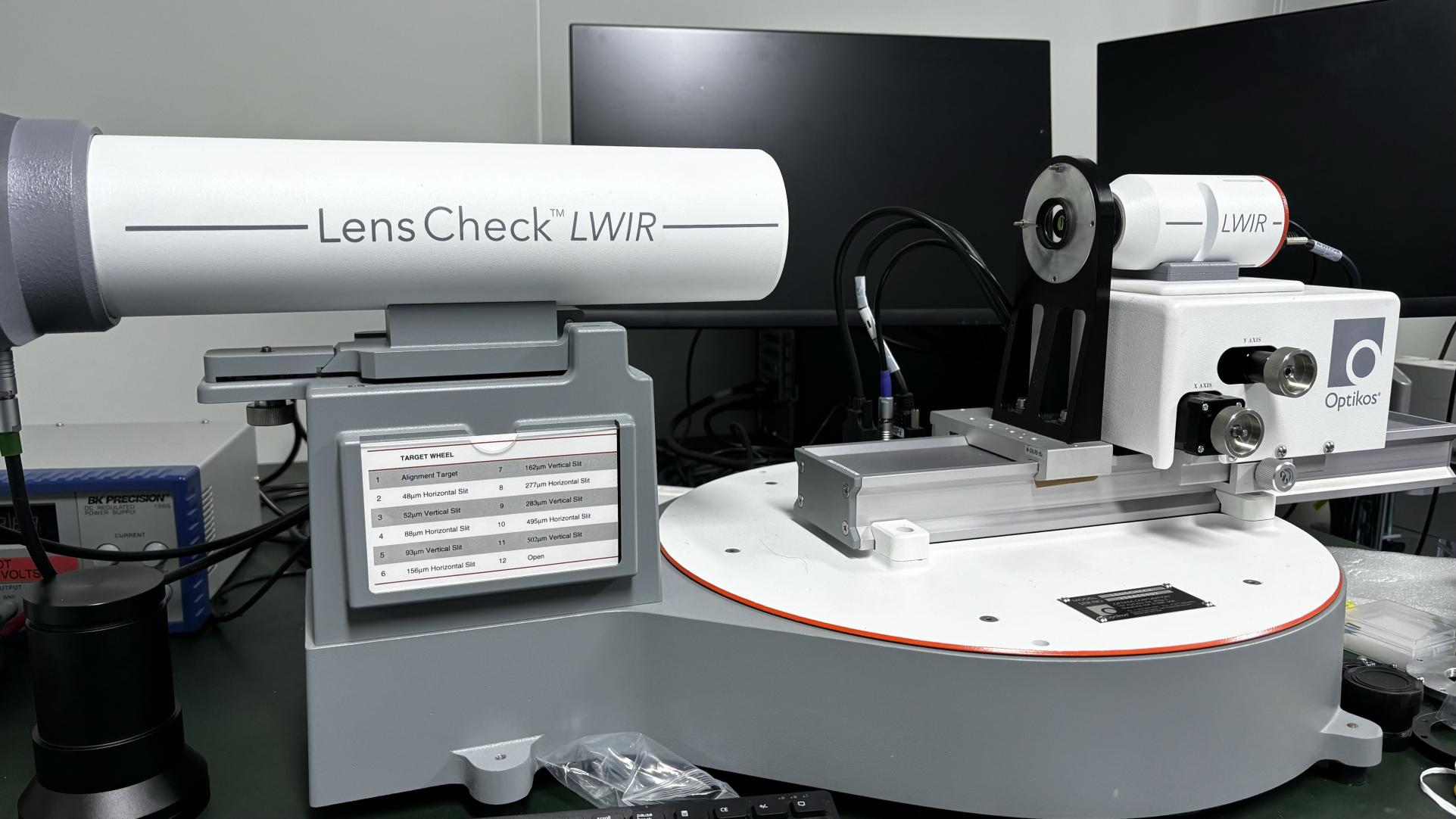
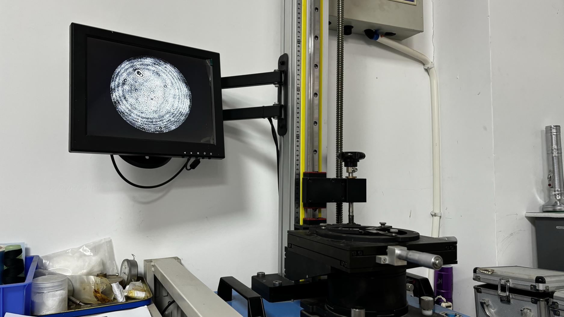
Our quality management workflow is built on strict redundancy. Every DSP assembly and memory module undergoes a comprehensive testing sequence including:
With an established network of more than 850 upstream and downstream suppliers, we minimize risk against global raw material disruptions. Whether sourcing active components, specific PCB copper formulations, or high-performance thermal interfaces, our robust supply network ensures continuous factory throughput and competitive lead times.


We specialize in turning custom specifications into production-ready physical components. Below is the workflow diagram of our OEM & ODM services:
Specification matching (low latency, specific clock rates, I/O protocols), thermal power budgets, and physical dimensions. Design validation begins here.
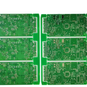
Multilayer PCB layout optimization, routing high-speed signal tracks to prevent crosstalk, and simulation of thermal dissipation and air flow dynamics.
Developing and flashing specialized BIOS, optimized memory-controller firmware, and providing baseline OS driver integration frameworks.
Entering international markets demands strict adherence to rigorous engineering, environmental, and safety standards. Our manufacturing and development processes are fully compliant with globally recognized frameworks, including RoHS, CE, FCC, and REACH certifications. This guarantees that all physical assemblies exported from our Chinese factories are fit for industrial deployment, commercial installation, or integration into medical-grade environments worldwide.
Furthermore, we maintain robust logistics integrations. From duty handling to secured shipping options, our export specialists manage the regulatory framework, documentation compliance, and custom clearance pathways. This seamless logistics pipeline guarantees that components arrive at integration sites across the Americas, Europe, or APAC regions with minimal delays and zero paperwork issues.
Technical and logistics answers for global system integrators and purchasing managers.
For standard memory module custom labeling or localized packaging modifications, our minimum order quantity starts at 100 units. For complete OEM/ODM custom PCB layouts, distinct silicon co-packaging, or specialized firmware optimization, the minimum runs begin at 500 to 1,000 units depending on the engineering complexity.
Signal integrity is maintained by employing premium low-loss, high-TG multi-layer PCBs (typically 8 to 12 layers). We use automated simulation software (such as HyperLynx) to layout differential lines, manage impedance profiles, minimize stub lines, and incorporate high-density power planes. This prevents cross-talk and jitter even under sustained 6000MHz operations.
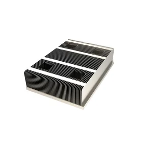
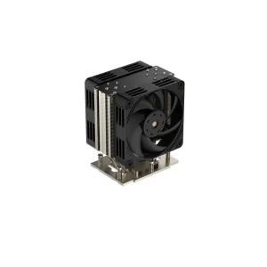
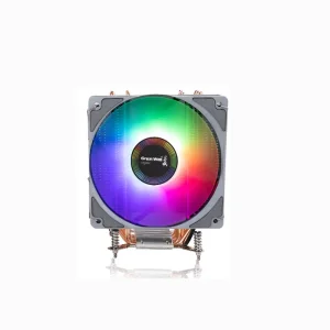
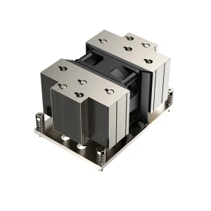
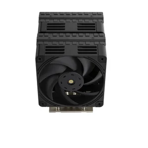
Yes. We design and manufacture specialized heatsinks including air-cooled multi-tube copper layouts, compact aluminum structures for server chassis (like SP3/SP5 and LGA4677 sockets), and custom vapor chambers. Each is simulated thermally to match the target heat load, ensuring system longevity.
Typically, schematic design and initial simulation take 2 to 3 weeks. Prototype PCB production and sample assembly require another 2 weeks. Functional testing, software adjustment, and customer validation samples are ready within 6 to 8 weeks from initial sign-off, followed immediately by volume mass production.